Solar Panel Manufacturing Techniques, Solar panel manufacturing typically begins with the production of silicon wafers, which are sliced from large cylindrical ingots through a process known as wafering.
The most common method for producing silicon wafers involves using a wire saw to cut thin slices from the ingot, minimizing material waste and maximizing efficiency.
After wafering, the silicon wafers undergo a surface treatment to remove impurities and create a smooth, uniform surface for the deposition of semiconductor materials.
The next step involves the application of thin layers of semiconductor materials, usually silicon, through techniques such as chemical vapor deposition (CVD) or physical vapor deposition (PVD), forming the solar cell structure.
Finally, the individual solar cells are interconnected, encapsulated, and assembled into solar panels, completing the manufacturing process. Continuous advancements in manufacturing techniques aim to enhance efficiency, reduce costs, and make solar energy more accessible on a global scale.
What Is Solar Panel?
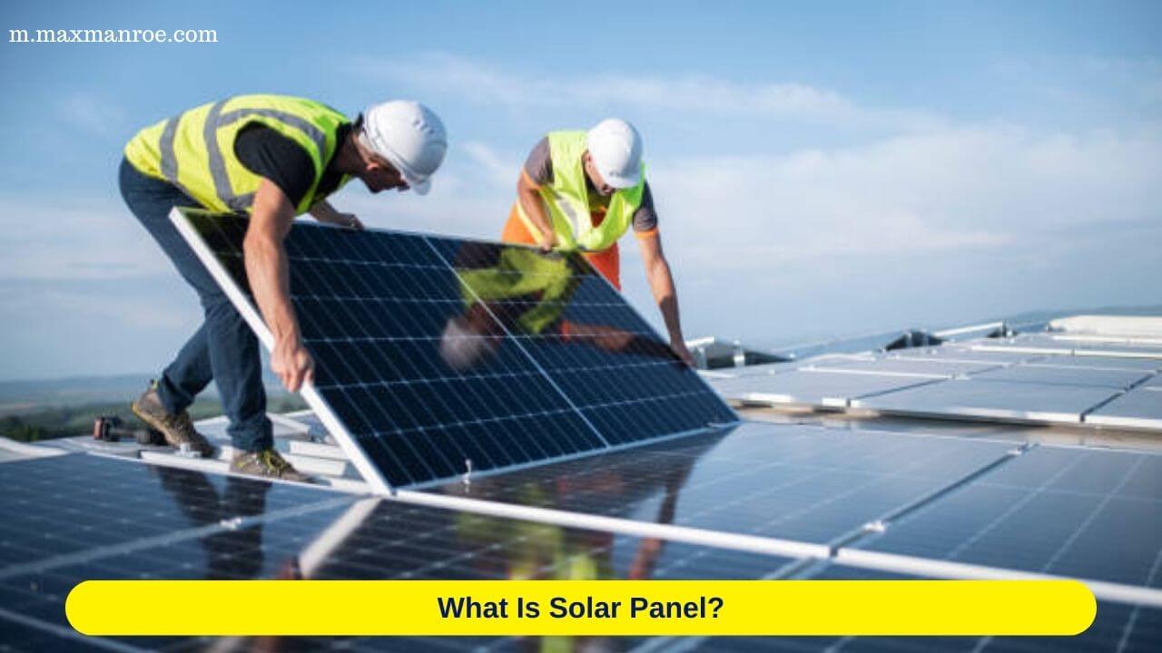
A solar panel, also known as a photovoltaic (PV) panel, is a device designed to convert sunlight into electricity.
It is a key component of solar photovoltaic systems, which harness the energy from the sun and convert it into usable electrical power.
Solar panels are made up of individual solar cells, typically composed of semiconductor materials, such as silicon.
When sunlight strikes these cells, it creates an electric current through the photovoltaic effect, generating direct current (DC) electricity.
This electricity can then be used to power various electrical devices or stored in batteries for later use.
Solar panels are a sustainable and renewable energy technology, playing a crucial role in the shift toward cleaner and more environmentally friendly sources of power.
They are commonly installed on rooftops, in solar farms, and even integrated into portable devices to harness solar energy for diverse applications.
Read More: Textile Machinery Manufacturers Guide 101: Types, Uses & Advancements in 2024
Solar Panel Manufacturing Techniques
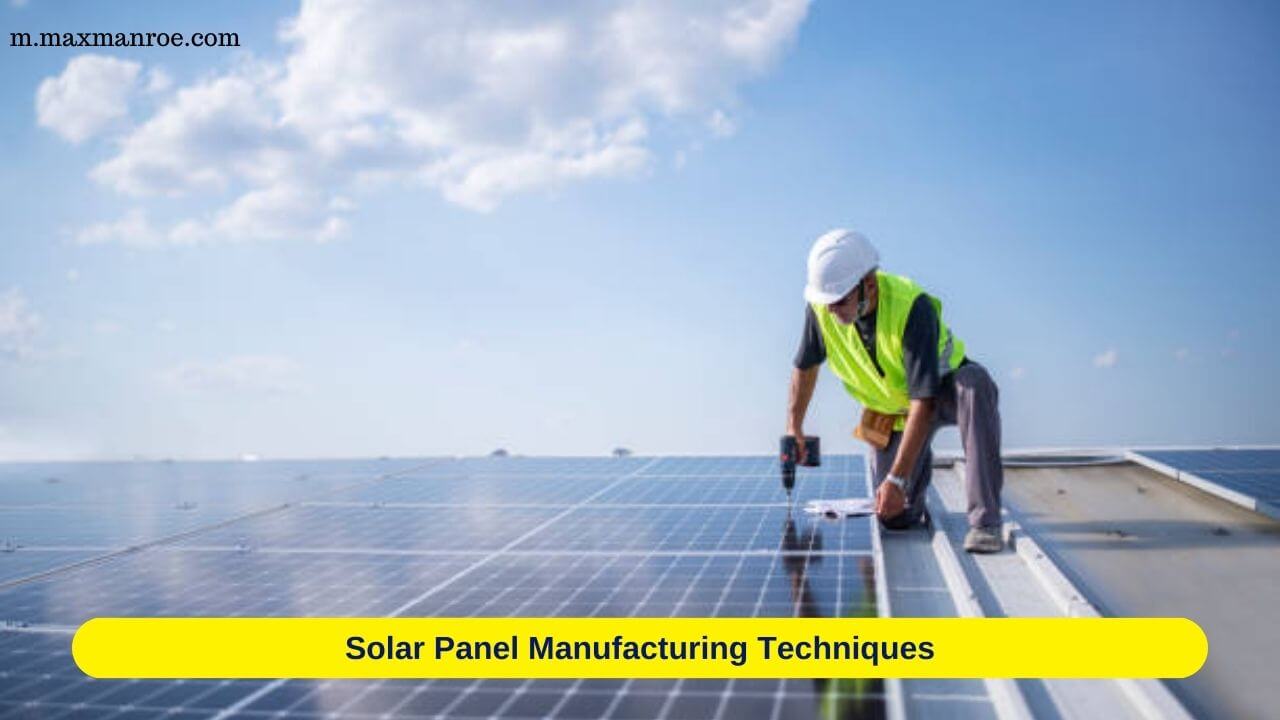
Solar panel manufacturing involves several key techniques to produce efficient and reliable photovoltaic modules.
Here are some of the main manufacturing techniques:
Wafer Production
Wafer production is a crucial step in the manufacturing of solar panels, semiconductors, and other electronic devices.
It involves the creation of thin, flat slices or wafers from a larger piece of material, typically a cylindrical ingot.
In the context of solar panels, wafer production specifically refers to the process of creating silicon wafers for use in solar cells.
Here is an overview of the wafer production process:
- Ingot Growth: High-purity silicon is melted and then solidified to form a cylindrical ingot. This ingot serves as the source material for the production of silicon wafers.
- Slicing (Wafering): The ingot is cut into thin slices, known as wafers, using a cutting technique. One of the common methods is wire sawing, where a wire with abrasive particles cuts through the ingot, creating multiple wafers. This process minimizes material waste and allows for the efficient use of the silicon.
- Surface Treatment: The sliced wafers undergo a surface treatment process to remove any impurities and contaminants. This treatment also smoothens the surface of the wafers, preparing them for the subsequent steps in the manufacturing process.
The resulting silicon wafers are then used as the substrate for the deposition of semiconductor materials and the creation of solar cells.
The quality of the wafer production process significantly influences the overall efficiency and performance of the solar panels.
Techniques for wafer production continue to evolve to enhance efficiency, reduce costs, and improve the overall sustainability of solar energy technologies.
Surface Treatment
The silicon wafers undergo a surface treatment process to remove impurities and create a smooth and uniform surface.
This treatment prepares the wafers for the deposition of semiconductor materials.
Deposition of Semiconductor Materials
Thin layers of semiconductor materials, commonly silicon, are deposited onto the surface of the wafers.
Techniques such as chemical vapor deposition (CVD) or physical vapor deposition (PVD) are used to create the necessary layers for the solar cell structure.
Solar Cell Fabrication
The treated and coated wafers are then processed to form individual solar cells.
Photolithography, which involves the use of light to transfer a pattern onto the solar cells, is often employed in this step.
Metal contacts are added to facilitate the flow of electrical current.
Interconnection and Encapsulation
The individual solar cells are interconnected to form a solar panel.
They are typically soldered together and then encapsulated in protective materials, such as tempered glass and polymer layers.
This encapsulation protects the solar cells from environmental factors and enhances the durability of the panel.
Assembly into Panels
Assembly into panels is the process where individual solar cells, which have been interconnected and encapsulated, are brought together to form a complete solar panel.
This step is a crucial part of the solar panel manufacturing process and involves several key activities:
Interconnection
The individual solar cells are interconnected to create a larger unit.
This is typically done by soldering or otherwise connecting the metal contacts on each cell to create a series or parallel arrangement, depending on the desired electrical characteristics of the panel.
Encapsulation
Before assembly, the interconnected solar cells are encapsulated to protect them from environmental factors such as moisture, dust, and physical damage.
This often involves placing the cells between layers of protective materials, such as tempered glass and polymer films.
The encapsulation process enhances the durability and longevity of the solar panel.
Frame Addition
Solar panels are often framed to provide structural support and protect the edges of the encapsulated cells.
The frame is usually made of aluminum or another durable material, and it adds rigidity to the overall structure.
Junction Box Installation
A junction box, containing electrical connections and possibly diodes for managing the flow of electricity, is added to the back of the solar panel.
This component facilitates the connection of the panel to an external electrical system.
Quality Control
After assembly, the solar panels undergo thorough quality control testing.
This includes electrical performance testing, visual inspections, and sometimes additional testing for factors like long-term durability.
Quality control ensures that the assembled panels meet industry standards and perform reliably over their intended lifespan.
Once the assembly into panels is complete and quality is assured, the solar panels are ready for distribution and installation.
They can be deployed in various settings, including residential, commercial, and utility-scale solar energy projects, contributing to the generation of clean and sustainable electricity.
Quality Control and Testing
Throughout the manufacturing process, rigorous quality control measures are implemented.
Testing includes electrical performance, visual inspections, and sometimes long-term durability testing to ensure the solar panels meet industry standards.
Continuous research and development in solar panel manufacturing aim to improve efficiency, reduce costs, and enhance the overall sustainability of solar energy technology.
Conclusion
In conclusion, solar panel manufacturing techniques involve a series of sophisticated processes aimed at transforming raw materials into efficient and durable photovoltaic modules.
The journey begins with the production of silicon wafers, sliced from cylindrical ingots through methods like wire sawing, optimizing material usage.
Surface treatment follows to ensure the wafers are free of impurities and provide a uniform foundation for the deposition of semiconductor materials.
The fabrication of solar cells involves precise techniques like photolithography and the addition of metal contacts to facilitate electricity flow.
The interconnected solar cells are encapsulated in protective layers, assembled into panels, and subjected to rigorous quality control measures.
Ongoing research and development focus on improving efficiency, reducing costs, and enhancing the sustainability of solar energy technologies, reflecting a continuous commitment to advancing clean and renewable energy solutions.